
Courtesy of RMIT University, Melbourne.
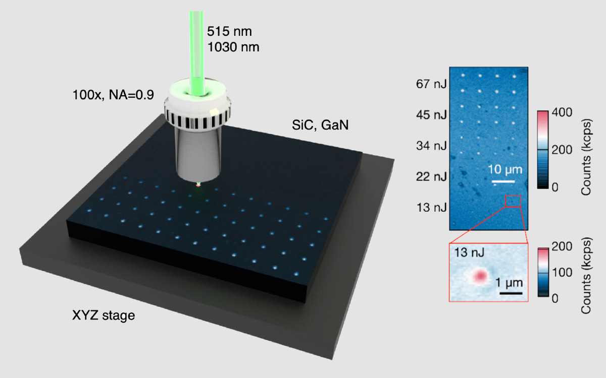
Color centers in wide bandgap semiconductors are relevant for quantum technologies as they can produce single-photon sources or be used as spin qubits and in quantum sensing applications. Femtosecond laser writing enables vacancy-related color centers writing in silicon carbide and gallium nitride, giving rise to photoluminescence from the visible to the infrared.
The process of color center creation is one of the point defects or point defect clusters associated with trapped electrons or holes in ordinarily transparent materials. When the electron ground state of the defect is excited to higher energy states by the absorption of laser light, these centers cause the solid to become colored.
Using a 515 nm wavelength 230 fs pulsed laser, RMIT University scientists produce large arrays of silicon-vacancy defects in silicon carbide with a high localization within the confocal diffraction limit of 500 nm and with minimal material damage. The number of color centers formed exhibited power-law scaling with the laser fabrication energy indicating that photoinduced ionization creates the color centers. Color center arrays play a crucial role in quantum applications.
Both femtosecond lasers PHAROS and CARBIDE can be applied to generate color centers in wide bandgap semiconductors.
- 190 fs – 20 ps 连续可调脉宽
- 最大输出 1 mJ @ 120 W 或 2 mJ @ 80 W
- 单脉冲 – 2 MHz 重复频率
- POD 和 BiBurst 功能
- 高达 5 次谐波或可调谐扩展
- 风冷型号
- 紧凑的工业级设计

- 100 fs – 20 ps 连续可调脉宽
- 最大单脉冲能量 4 mJ
- 最小脉宽输出 < 100 fs
- POD 和 BiBurst 功能
- 高达 5 次谐波或可调谐扩展
- CEP 稳定或重复频率锁定
- 热稳定性和密封设计
Highly Emissive Deep-Red Perovskite Quantum Dots in Glass: Photoinduced Thermal Engineering and Applications
K. Sun, D. Tan, J. Song, W. Xiang, B. Xu, and J. Qiu, Advanced Optical Materials, 2100094 (2021).
Photoluminescence of Point Defects in Silicon Dioxide by Femtosecond Laser Exposure
V. D. Michele, E. Marin, A. Boukenter, M. Cannas, S. Girard, and Y. Ouerdane, physica status solidi (a), 2000802 (2021).
Color Centers Enabled by Direct Femto-Second Laser Writing in Wide Bandgap Semiconductors
S. Castelletto, J. Maksimovic, T. Katkus, T. Ohshima, B. C. Johnson, and S. Juodkazis, Nanomaterials 1 (11), 72 (2020).
Laser writing of color centers in silicon carbide
S. Castelletto, T. Katkus, and S. Juodkazis, in SPIE Micro + Nano Materials, Devices, and Applications 2019, M. C. Simpson, and S. Juodkazis, eds. (SPIE, 2019).
Photoluminescence in hexagonal silicon carbide by direct femtosecond laser writing
S. Castelletto, A. F. M. Almutairi, K. Kumagai, T. Katkus, Y. Hayasaki, B. C. Johnson, and S. Juodkazis, Optics Letters 24 (43), 6077 (2018).
Fluorescent color centers in laser ablated 4H-SiC nanoparticles
S. Castelletto, A. F. M. Almutairi, G. Thalassinos, A. Lohrmann, R. Buividas, D. W. M. Lau, P. Reineck, S. Juodkazis, T. Ohshima, B. C. Gibson et al., Optics Letters 7 (42), 1297 (2017).
Analysis of defects patterned by femtosecond pulses inside KBr and SiO2 glass
X. W. Wang, R. Buividas, F. Funabiki, P. R. Stoddart, H. Hosono, and S. Juodkazis, Applied Physics A 3 (122) (2016).
Engineering and Localization of Quantum Emitters in Large Hexagonal Boron Nitride Layers
S. Choi, T. T. Tran, C. Elbadawi, C. Lobo, X. Wang, S. Juodkazis, G. Seniutinas, M. Toth, and I. Aharonovich, ACS Applied Materials & Interfaces 43 (8), 29642-29648 (2016).